But there is still a way out. This is an ordinary, standard ATX from any, even the simplest and most ancient computer. Despite the cheapness of such power supplies (second-hand ones can be found from companies and for 5e), they provide very decent current and universal voltages. On the +12V line - 10A, on the -12V line - 1A, on the 5V line - 12A and on the 3.3V line - 15A. Of course, these values are not exact and may vary slightly depending on specific model ATX PSU.

Just recently I did one interesting thing- a music center made from the housing of a small speaker. Everything would be fine, but given the decent power of the bass amplifier, the current consumption of the center in the bass peaks reached 8A. And even an attempt to install a 100-watt transformer with 4-amp secondary power supply did not give a normal result: not only did the voltage drop by 3-4 volts in the bass (which was clearly visible from the attenuation of the backlight lamps on the front panel of the radio), but also There was no way to get rid of the 50Hz background. At least set it to 20,000 microfarads, or at least shield everything you can.
And just as luck would have it, the old system unit burned out at work. But the block ATX power supply still working. So we'll plug it in for the radio. Although according to the passport, car radios and their amplifiers are powered by a voltage of 12V, we know that it will sound much more powerful if 15-17V is applied to it. At least in my entire history, not a single receiver has ever burned out from an extra 5 volts.

Since in the existing ATX power supply the voltage of the 12-volt bus was only a little more than 10V (maybe that’s why the system unit didn’t work? It’s too late), we will raise it by changing the control voltage on the 2nd pin of the TL494. See the schematic diagram of a computer power supply here.

Simply put, we’ll change the resistor or even solder it onto tracks of a different value. I set two kilo-ohms and 10.5V turns into 17. Do you need less? - We increase the resistance. Starts computer unit power supply by shorting the green wire to any black one.

Since the places in the building of the future music center not much - we take out the ATX switching power supply board from its original case (the box will be useful for my future project), and thereby reduce the dimensions of the power supply by half. And don’t forget to resolder the filter capacitor in the power supply to a higher voltage, otherwise you never know...


What about the cooler? - An attentive and smart radio amateur will ask. We don't need him. Experiments showed that with a current of 5A 17V during an hour of operation of the radio at maximum volume (don’t worry about your neighbors - two 4 Ohm 25 watt resistors), the radiator of the diodes was a little warm, and the radiator of the transistors was almost cold. So such an ATX power supply will handle a load of up to 100 watts without problems.
Discuss the article SIMPLE ATX POWER SUPPLY
Actually, the idea of making a laboratory power supply with adjustable output voltage and current from a computer one is not new. There are many options for such modifications on the Internet.
The advantages are obvious:
1. Such power supplies are literally “lying under your feet.”
2. They contain all the main components, and most importantly, ready-made pulse transformers.
3. They have excellent weight and size characteristics - such a transformer power supply would weigh more than 10 kg (this one is 1.3 kg in total).
True, they are not without their disadvantages:
1. Due to pulse conversion, the output voltage contains a rich spectrum of high-frequency interference, which makes them of limited applicability for powering radio stations.
2. They do not guarantee a low output voltage (less than 5 V) at low load currents.
And, nevertheless, such a power supply is perfect for powering automotive electronics at home, when testing and debugging electronic devices. And the presence of a current stabilization mode allows it to be used as a universal Charger for a wide range of batteries!
Output voltage - from 1 to 20 V
Output current - up to 10 A
Weight 1.3 kg

First, let's figure out which power supplies are suitable for conversion. Best for laboratory block For power supply, just old AT or ATX power supplies assembled on a TL494 PWM controller (aka: μPC494, μA494, UTC51494, KA7500, IR3M02, MV3759, etc.) with a power of 200 - 250 W are suitable. Most of them are like this! Modern ATX12B, 350 - 450 W, of course, is also not a problem to remake, but they are still better suited for power supplies with a fixed output voltage (for example, 13.8 V).
To further understand the essence of the modification, consider the principle of operation of the power supply for a computer.
More or less standardized power supplies (PC/XT, AT, PS/2) for computers appeared in the early 80s thanks to IBM, and existed until 1996. Let's look at their operating principle according to the structural diagram:
![]()
AT power supply block diagram
The mains voltage is supplied to the power supply through an electromagnetic interference filter, which prevents the spread of high-frequency interference from the pulse converter to the supply network. This is followed by a rectifier and a smoothing filter, the output of which is a constant voltage of 310 V. This voltage is supplied to a half-bridge inverter, which converts it into square pulses and feeds it to the primary winding of step-down transformer T1.
Voltages from the secondary windings of the transformer are supplied to rectifiers and smoothing filters. As a result, at the output we obtain the necessary constant voltages.
When power is applied, at the initial moment, the inverter starts in self-generation mode, and after voltage appears on the secondary rectifiers, the PWM controller (TL494) is switched on, which synchronizes the operation of the inverter by supplying trigger pulses to the bases of the key transistors through the decoupling transformer T2.
The power supply uses pulse-width regulation of the output voltage. To increase the output voltage, the controller increases the duration (width) of the trigger pulses, and to decrease it, it decreases it.
Stabilization of the output voltage in such power supplies is often carried out using only one output voltage (+5 V, as the most important), sometimes two (+5 and +12), but with priority +5 V. For this, the input of the controller comparator ( pin 1 of TL494, output voltage is supplied through the divider. The controller adjusts the width of the trigger pulses to maintain this voltage at the required level.
Also, the power supply has 2 types of protection system. The first is from exceeding the total power and short circuit, and second, from overvoltage at the outputs. In case of overload, the circuit stops the pulse generator in the PWM controller (by supplying +5 V to pin 4 of the TL494).
In addition, the power supply contains a node (not shown in the diagram) that generates the POWER_GOOD signal (“voltage is normal”) at the output after the power supply reaches an operating mode that allows the processor to start in the computer.
The AT power supply (PC/XT, PS/2) has only 12 main wires for connecting to motherboard(2 connectors with 6 contacts each). In 1995 Intel company I was horrified to discover that existing power supplies could not cope with the increased load, and introduced a standard for a 20/24-pin connector. In addition, the power of the +3.3 V stabilizer on the motherboard to power the processor was also no longer enough, and it was moved to the power supply. Well, Microsoft introduced operating system Windows, Advanced Power Management (APM) power management modes... Thus, in 1996, the modern ATX power supply appeared.
Let's look at the differences between the ATX power supply and the old AT according to its structural diagram:

Block diagram of an ATX power supply
The Advanced Power Management (APM) mode required the abandonment of the mains switch and the introduction of a second pulse converter into the power supply - a standby voltage source of +5 V. This low-power power supply always works when the mains plug is plugged into the network. The primary voltage comes from the same rectifier and filter as the main inverter.
In addition, power to the PWM controller in ATX comes from the same standby source (not stabilized 12 - 22 V), and there is no autostart of the inverter. Therefore, the power supply starts only if there are start pulses from the controller. The main power supply is turned on by turning on the pulse generator of the PWM controller with the PS_ON signal (shorting it to ground) through a protection circuit.
That's all the main differences.
How to choose a power supply for conversion?
As you know, power supplies are made in China. And this may entail the absence of some components that they considered “superfluous”:
1. There may be no EMI filter at the input. The most important thing in the filter is the inductor wound on a ferrite ring. Usually, it is clearly visible through the fan blades. Instead, there may be wire jumpers. The presence of a filter is an indirect sign of a high-quality power supply!
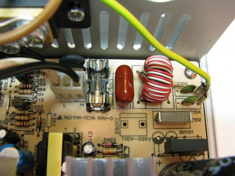
EMI filter elements
2. Also, you need to look at the size of the step-down transformer (the larger one). The maximum power of the power supply depends on it. Its height should be at least 3 cm. There are power supplies with a transformer less than 2 cm high. The power of these is 75 W, even if it says 200.
3. To check the functionality of the power supply, connect a load to it. I use car headlight bulbs with a power of 50 - 55 W and a voltage of 12 V. Be sure to connect one to the +5 V circuit (red wire), and the second to the +12 V circuit (yellow wire). Turn on the power supply. Disconnect the fan connector (or, if the Chinese saved on it, just stop it with your hand). The power supply should not beep.
After a minute, unplug it and feel with your hand the temperature of the radiators and the group filtration choke in the filter secondary stresses. The throttle should be cold, and the radiators should be warm, but not hot!
I used a power supply from 1994 with a power of 230 W - they didn’t save money back then.
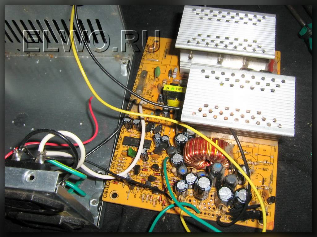
Reworking the power supply
You need to start by cleaning the power supply from dust. To do this, disconnect (unsolder) the network wires and wires to the 110/220 switch from the board - we will no longer need it, because in the 220 V position the switch is open. Remove the board from the case. Vacuum cleaner, hard brush, and go!
Next, you need to try to find an electrical schematic diagram your power supply, or at least as similar as possible to it (they do not differ significantly). It will help you navigate the values of the “missing” components. I do not rule out that, like me, you will have to copy some components from the board.

EMI filter circuit, rectifier and filter primary voltage, and the inverter after modification
The values of the replaced components are highlighted in red in the diagram. Newly installed components have positional designations highlighted in red.
1. Check that all capacitors and inductors are present in the EMI filter. If missing, install them (I only had C2 missing). I also installed a second, additional noise filter, made in the form of a socket for connecting the power cord.
2. Look at the types of diodes used in the rectifier (D1 - D4). If there are diodes with a current of up to 1 A (for example, 1N4007) - replace them with at least 2 A, or install a diode bridge. I had a 2-amp bridge.
3. In the vast majority of power supplies, capacitors with a capacity of no more than 200 μF (C5 - C6) are installed in the primary voltage filter. To deliver full power, replace them with capacitors with a capacity of 470 - 680 μF, suitable in size, with a voltage of at least 200 V. Preference should be given to the 105 ° C group.
4. Transistors in a half-bridge inverter (Q1, Q2) can be very diverse. In principle, most of them are not heated criminally. To reduce heating, they can be replaced with more powerful ones - for example, 2SC4706, installing them on a radiator through insulating gaskets. I went even further and replaced both radiators with more efficient ones.
5. While testing the power supply under maximum load, capacitor C7 heated up and burst (usually 1 µF 250 V). This capacitor should not get hot at all. I think it was faulty, but I still replaced it with 2.2 uF 400 V.
Now let's consider block diagram converted power supply:

Block diagram of a laboratory power supply
To modify, we will need to remove all the secondary rectifiers except one (although replacing almost all the components in it), redo the protection circuit, add a control circuit, a shunt and measuring instruments. Elements of the POWER_GOOG schema can be deleted. Now more details.
To remove the output voltage, the 12-volt winding of the step-down transformer T1 is used. But it is more convenient to install the rectifier and filter in place of the 5-volt one - there is more space for diodes and capacitors.
The secondary voltage rectifier and filter, after modification, should look like this:

Secondary voltage rectifier circuit after modification
1. Unsolder all elements of rectifiers and filters +5, +12 and -12 V. With the exception of damper circuits R1, C1, R2, C2 and R3, C3 and inductor L2. Subsequently, with an output voltage of about 20 V, I noticed resistor R1 heating up and replaced it with 22 Ohms.
2. Cut the tracks leading from the 5-volt taps of the transformer winding T1 to the +5 V rectifier diode assembly, while maintaining its connection to the -5 V rectifier diodes (we will need it later).
3. In place of the diode assembly of the +5 V rectifier (D3), install an assembly on Schottky diodes for a current of 2x30 A and a reverse voltage of at least 100 V, for example, 63CPQ100, 60CPQ150. (The standard 5-volt diode assembly has a reverse voltage of only 40 V, and the standard diodes in the 12 V rectifier are designed for too low a current - they cannot be used.) This assembly practically does not heat up during operation.
4. Connect the terminals of the 12-volt winding with the installed diode assembly using thick wire jumpers. The damper circuits R1, C1 connected to this winding are saved.
5. In the filter, instead of the standard ones, install electrolytic capacitors (C5, C6) with a capacity of 1000 - 2200 μF for a voltage of at least 25 V. And also add ceramic capacitors C4 and C7. Install instead of the standard one, load resistor 100 Ohm, power 2 W.
6. If, when checking the power supply under load, the group filtering choke (L1) did not heat up, then just rewind it. Wind all the windings from it, counting the turns. (Usually, 5 V windings contain 10 turns, and 12 V windings contain 20 turns.) Wind a new winding with two wires folded together with a diameter of 1.0 - 1.3 mm (similar to a standard 5 volt one) and a number of turns of 25-27.
If the inductor was heated, then its core is damaged (powdered iron has such a problem - it “sinters”), then you will have to look for a new core made of powdered iron (not ferrite!). I had to buy a ring core white slightly larger diameter and wind a new winding. It doesn't heat up at all.
7. Choke L2 remains standard, from a 5-volt filter.
8. To power the fan, a 5-volt winding is used, and the rectifier wiring is -5 V, which we convert to +12. The standard diodes are used, from the -5 V rectifier (D1, D2), they must be soldered with reverse polarity. The choke is no longer needed - solder the jumper. And in place of the standard filter capacitor, install a capacitor with a capacity of 470 uF 16 V, of course, with reverse polarity. Throw a jumper from the filter output (formerly -5 V) to the fan connector. Directly near the connector, install a ceramic capacitor C9. The voltage on my fan is +11.8 V, and at low load currents it decreases.
9. In the power supply circuit of the PWM controller (Vcc), it is necessary to increase the capacitance of filter capacitors C10 and C11. The voltage from capacitor C10 (Vdd) is used to power the digital ammeter and voltmeter.
The protection circuit for exceeding the total power remains unchanged. Only the output overvoltage protection circuit is changed. Here is the final diagram:

Scheme of the protection unit after modification
When the load on the inverter increases above the permissible limit, the pulse width at the middle terminal of the isolation transformer T2 increases. Diode D1 detects them, and the negative voltage across capacitor C1 increases. Having reached a certain level (approximately -11 V), it opens transistor Q2 through resistor R3. A voltage of +5 V will flow through an open transistor to pin 4 of the controller and stop the operation of its pulse generator. In your power supply, such protection may be organized differently. In any case, you don't need to touch it.
All diodes and resistors suitable from the secondary rectifiers to the Q1 base are unsoldered from the circuit, and a zener diode D3 is installed for a voltage of 22 V, for example, KS522A, and resistor R8.
In the event of an emergency increase in voltage at the output of the power supply above 22 V, the zener diode will break through and open transistor Q1. This, in turn, will open transistor Q2, through which a voltage of +5 V will be supplied to pin 4 of the controller, and will stop the operation of its pulse generator.
All that remains is to assemble the control circuit and connect it to the PWM controller.
The control circuit consists of two amplifiers (current and voltage), which are connected to the standard inputs of the controller error comparators. He has 2 of them (pins 1 and 16 of TL494) and they work via OR. This allows you to obtain both voltage and current stabilization. Final control unit diagram:

Control unit diagram
The operational amplifier DA1.1 is used to assemble a differential amplifier in the voltage measurement circuit. The gain is selected in such a way that when the output voltage of the power supply changes from 0 to 20 V (taking into account the voltage drop across the shunt R7), the signal at its output changes within 0...5 V. The gain depends on the ratio of the resistances of resistors R2/R1 =R4/R3.
Please note: for correct voltage measurement, resistors R1 and R3 are connected with separate thin wires directly to the output voltage connecting terminals.
The operational amplifier DA1.2 is used to assemble an amplifier in the current measurement circuit. It amplifies the magnitude of the voltage drop across shunt R7. The gain is selected in such a way that when the load current of the power supply changes from 0 to 10 A, the signal at its output changes within 0...5 V. The gain depends on the ratio of the resistances of resistors R6/R5.
As a current sensor (R7), I used a standard 75SHIP1500.5 measuring shunt with a fairly low resistance of 1.5 mOhm. Therefore, in the measurement circuit I also included the connecting wires that connect the shunt. This made it possible to eliminate the differential amplifier and reduce the number of wires. Resistor R5 is connected directly to ground near the op-amp, and the non-inverting input (pin 5) is connected to the same wire (from R3) going to the negative terminal.

Measuring shunt 75SHIP1500.5
When using a shunt with a different resistance and with a different length of connecting wires, you will need to select resistor R5 so that the maximum stabilization current corresponds to 10 A.
Signals from both amplifiers (voltage and current) are supplied to the inputs of the error comparators of the PWM controller (pins 1 and 16 of DA2). To set the required voltage and current values, the inverting inputs of these comparators (pins 2 and 15 of DA2) are connected to adjustable reference voltage dividers (variable resistors R8, R10). The +5 V voltage for these dividers is taken from the internal reference voltage source of the PWM controller (pin 14 of DA2).
Resistors R9, R11 limit the lower adjustment threshold. Capacitors C2, C3 eliminate possible “noise” when turning the variable resistor motor. Resistors R14, R15 are also installed in case of a “break” of the variable resistor motor.
A comparator is assembled on the operational amplifier DA1.4 to indicate the transition of the power supply to current stabilization mode (LED1).
In the circuit I used a quad LM324A operational amplifier, but you can use others that operate over a wide range of supply voltages, for example, two dual LM358s. Power to it (Vcc) is supplied from the power circuit of the PWM controller (from pin 12 of DA2) which varies within 5...25 V, depending on the output voltage of the power supply.
Adjustment elements R8 - R11, as well as capacitors C2 and C3, are located on a small board screwed to the front panel of the power supply. All other elements of the circuit are located in free space printed circuit board power supply.

To connect amplifiers to a PWM controller (DA2), you must first unsolder all standard components going to pins 1, 2, 3, 15 and 16 from it.
To measure and display the output voltage and current, I used a ready-made digital voltmeter and ammeter, connected according to the circuit according to the instructions supplied with them. Power is supplied to them from capacitor C10 (see diagram of secondary rectifiers). If you have an ATX power supply with a standby power supply at your disposal, then supply power to the meters (Vdd) from this source - it has an unstabilized voltage output of +12 - 22 V.
To connect these devices, it is convenient to use the connectors for Floppy drives available on the standard cables of the AT power supply.
Please note that the measuring leads of the voltmeter are connected with separate thin wires directly to the output terminals of the power supply. And the measuring leads of the ammeter go directly to the measuring contacts of the shunt.
Part of the standard metal case (bottom and side wall) of the power supply in my design serves as a chassis for the board and for the shunt.
To reduce the level of high-frequency interference, ceramic capacitors with a capacity of 1 μF are located directly at the output terminals (C6, C7 in the control unit diagram).
 |
 |
 |
 |
For my power supply, I used a ready-made case with a carrying handle. A Ø50 mm fan is used for cooling. It drives air inside the housing. To do this, the necessary hole was cut in the case opposite the radiators, and on the opposite side and back wall, holes were drilled for air outlet. Design ideas depend only on your taste.
If you intend to use such a power supply for radio stations, then I strongly recommend keeping the standard one in the design metal case- it perfectly screens and reduces the level of electromagnetic interference emitted by the inverter.
Full description of power supplies from computers and operating modes.
This article used only facts that have been verified and tested by time. The author of the article does not set out to convince the reader of anything. And even more so does not bear any responsibility for your experiments with your own equipment. The information is valid for power supplies costing much less than $40. So. Let's go back to our... uh... file servers and routers. As a rule, in home networks such a thing does not belong to a specific person, but is assembled from common components or with common money. They try to make it reliable and cheaper (CPU - Intel, Memory - no more, no less, network drives - NE2000 ISA 10Base2/T). For complete reliability and speed, Unix is installed on all this hardware. Oh yes!!! I completely forgot. UPS is also needed here.
Without the cost of UPS, a modest system will cost $50..70 + the cost of a HDD for a file server. Naturally, the power supply in such a system cannot cost $40
Someone will object: “And we have an old case from the brand i486.” Yes. How old is this PSU? And how many more years will he have to work? Will all this work for a long time and without glitches? So:
Typical circuit diagram of an AT 200W power supply.
The main disadvantage of all cheap power supplies
This is what the +5V voltage oscillogram of a cheap power supply looks like.
Fig1. Static load 30% 
In general, everything is within normal limits. Short voltage surges are noticeable. With increasing load, emissions increase. The consequence is glitches in memory and other digital elements of the PC. Note that the load is 30% - this is the majority of PCs not burdened with more than one HDD. Those who have a simple video card and a CPU that consumes no more than 15W.
Second drawback
In theory, it is said that UPSs are very critical to the instability of the load current. In our case, this drawback manifests itself in all its glory. This is what the +12V voltage oscillogram looks like under a dynamic load.
Fig2. Combined load 50% (2 or more HDDs) 
In Fig. 2, section No. 1 is a static load. Section No. 2 is HDD in read/write mode. Characteristic dips in the +12V supply voltage. The magnitude and duration of the dip depends on the filter parameters of the power supply and the power of the HDD. Consequence: Due to instability of the +12V power bus HDD starts slapping their heads on the “pancakes”. Bad things appear. Glitches in devices powered by the +12V bus (ISA cards, COM ports)
How to deal with it
Consider the power supply filter.
Fig3. Filter (what it is) 
In most AT units, the filter for the +5V power bus consists of two 1000µFx10V electrolytic capacitors. For the +12V power bus, one capacitor is 1000μFx16V. For switching power supplies, the capacitance of the filter capacitors is taken at the rate of 500..1000 µF per 1A load current. In our case, we obtain for the +5V bus the maximum load current will be 4A. For the +12V power bus, the maximum load current will be 2A. In most cases, an emergency does not occur. But when using even one HDD of the IBM DPTA 7200RPM type (or with similar power consumption), the above glitches were observed.
Fig4. Filter. (what it should be) 
For this circuit (Fig. 4.) the following parameters are valid: +5V bus – maximum dynamic load current 20A. +12V bus – maximum dynamic load current 8A. Electrolytic capacitors eliminate current instability. Ceramic capacitors (2.2 µF 3..6 pcs.) eliminate pulsed voltage surges. A series with low resistance for pulsed currents is recommended (I think that’s what it’s called) Each company labels them differently. From what you can get in St. Petersburg - for example, Hitano, EXR Series, operating temperature up to 105 Celsius. For +5V - two things 2200 µF or 3300 µF 6.3 or 10 V (you need to look at the dimensions, power supply manufacturers squeeze the space very much) I can’t advise anything with ceramics. From what I have seen, only TKE and accuracy differ (for example + 80 -50%) .I think this is not important in filters of this kind. Here, the larger the capacity, the better. It's probably better to take SMD (unpackaged) and solder from the back of the board directly onto the conductors. Regarding the coils in the output filters: If you don't have winding experience, it's better not to experiment. If you can buy it, you can try it. Or unsolder it from a dead power supply. With coils at the output, you need to be very careful. Check the block only by loading it on resistors. After upgrading the filter, look at the oscillogram.
Fig5. Static load 30% (+5V bus) 
This is what the voltage “surface” of a branded power supply looks like under load. There are voltage surges, but they are insignificant (much less than the permissible norm) and practically do not increase with increasing load. The total capacity (my version) of electrolytic capacitors is 6800 μF. Ceramic capacitors 1.5uF. (everything that was at hand). For interest, the block was tested ATX power supply from PowerMan from the InWin A500 case - the oscillogram is similar, but there are no voltage surges.
Fig6. Combined load 50% (2 or more HDDs) 
In Fig. 6, section 2 corresponds to dynamic load.
The filter capacity is one capacitor 4700 μFx25V (HDD in read/write mode). The maximum interference is no more than 100 mV. The PowerMan ATX power supply showed approximately the same result.
Circuit circuit resistance 220V - mains voltage. (220V)
It is not difficult to guess that the numerator is always greater than the denominator.
On the oscillogram (Fig. 9) section 2 - there is a “dip” in the mains voltage lasting 20..500 ms. (Typical for connecting consumers with a reactive nature of resistance to the network) The UPS saves you from short voltage dips. (minimum turn-on time of the uninterruptible power supply is 4 ms) This is good if he is. It may be necessary to increase the capacity of the high voltage DC filter. (in Fig. 10 - electrolytes 680x250V). Usually 220x200V are installed. With a power consumption of 100 Watt, the reserve capacity (220x200V) is enough for 70..100 ms. If you increase the capacity to 680..1000μFx200V, then do not forget to replace the RS205 (2A 500V) diode assembly with RS507 (5A 700V). A thermistor is required. 4.7 ... 10 Ohm at 10A. They usually save money on thermistors. Set the usual resistance 1 Ohm 1 Watt
Fig. 10. Network filter+ rectifier. What they should be. 
Of all the elements in the filter circuit of a conventional power supply, only the PS405L thermistor and fuse are present. (the most necessary) Sometimes they install a symmetrical transformer (5mH in the diagram). Of course - RS205 rectifier and high-voltage DC filter (2 electrolytes 220x200V)
Increased efficiency
1 Replacing powerful key transistors.
We will be replacing the imported bipolar KSE13007 (or NT405F, 2SC3306) with our Soviet field device KP948A.
Fig. 11 Typical connection circuit for a field-effect transistor. 
This option is suitable for ATX power supplies, because The block is started from a separate low-power power source. For AT blocks, such a circuit is not suitable. Therefore, I left the transistor wiring as is, adding a 15V zener diode. (as shown in the diagram in Fig. 11) It is not necessary to install zener diodes, because the forward voltage at the gate does not exceed 1V (direct diode), and its reverse breakdown voltage does not exceed 10V. Capacitors 1 * 50v (Fig. 12.) should be installed ceramic (if the goal is to increase reliability), these electrolytes dry out (especially next to a hot radiator) is the main reason for the failure of the power supply, since the power transistors are not turned off sharply enough.
I don’t know why, but it works for me. The power drop on the transistors decreases by 3..5 Watts. Although I still left the zener diodes. As a result, it stops heating.
 <
<
2 Rectifier diodes.
We install powerful rectifier diodes on normal radiators. If a CPU radiator is suitable, we cut it in half. One half is a +5V rectifier. The second is for the +12V rectifier. It is also recommended to replace the power diode assemblies with our Soviet KD2998A diodes. Radiators - enlarge. All! Now you can remove the fan from the power supply. This disrupts the normal heat exchange inside the case. But if this is a power supply for a router, then there’s nothing special to heat up inside the case. If this is a file server - then at your own peril and risk. Although Manowar Manowar claims that he has a converted ATX power supply loaded with 2HDD 7200RPM + ULF and the whole thing works without a fan.
Suddenly winter came and it got cold outside. And then they poured in the wrong kind of gasoline. In general, the king of the German automobile industry stood up, somewhere near Moscow, just like his older “profathers” did 67 years ago. The battery ran out, so we continued on foot.... To charge the battery at home, we only found a couple of burnt-out ATX units. I’ll immediately add that this “charging” is not intended for restoration, desulfation and other unpromising shamanic methods, which our fathers (including myself) did in a past life due to the extreme wretchedness of life.
This is simply a unit that allows you to reliably and at the lowest cost charge a dead but serviceable battery. Its essence is simple and clear. It produces an output charging current of about 5-6 Amperes, with any active load, up to a short circuit. In this case, the output voltage will under no circumstances exceed the specified value. I set it to 14.6 volts.
First you need to get the block working
In order for "dummies" about restoring blocks, general rules:

The frequency of the internal oscillator is determined by the formula:
where R and C are the resistor and capacitor on pins 6 and 5, respectively, that is, they cannot be cut.
Pin 14 is the output of the internal +5 volt reference voltage.
Pins 1,2,15 and 16 are the inputs of 2 built-in comparators, which the user can use at his discretion, i.e. control the width of the PWM output pulses. Both comparators are exactly the same, with the only difference being that the comparator with pins 15-16 operates with a “delay” of 80 mV. In the ATXs I received, this comparator was not used, pin 16 is grounded, and pin 15 is connected to Uref, i.e. 14 output.
Pin 13 is intended for switching the TL-494 into control mode for flyback single-ended converters. In this case, the “dead time” can be increased to 96%. In our “push-pull” case, this pin is also connected to Uref.
We will use the comparator on pins 1-2 to set the output voltage; for this, we apply part of Uref to pin 2, which is done in most AT and ATX. Typically this voltage is approximately 2.5 volts, i.e. with Uref (+5Volt) through a resistive divider.
The RC chain from pin 2 to pin 3 (FB or OS) is designed to limit the PWM speed while stabilizing the voltage and is available in all AT-ATX circuits. It also cannot be cut out.
I am drawing a simplified output voltage control circuit.
The voltage at the power supply output will be equal to Uout=Uref1(1+Roc/Rm) . Now you must decide for yourself, with a calculator in your hands, which resistors to make up the divider from. I did it as shown in the diagram. Be sure to check, if this formula doesn’t work for you, it means you haven’t cut everything. It is important to take into account that without rewinding the transformer you will not be able to get more than 18-20 volts at the 12-volt output. In principle, a power supply can provide up to 24 volts, but this is in the absence of load and a completely “open” PWM, that is, when the “dead” time is no more than 4% of the period. Without a throttle, the power supply will not feel very comfortable. It will be difficult for him to maintain the output voltage. It will “squash and wobble” like a car with a jammed shock absorber. Our goal is to achieve a limit of 14.6-14.8 Volts. For “dead” batteries, a voltage of up to 16 (or more) volts is required. For recovery fans, you can get that much.
For dessert, a little about pin 4.
This is also a comparator input, but with a delay of 120 mV. And here it’s not even a matter of delay, but the fact that the chip designer foresaw to use it to adjust the “dead time”. Usually in ATX-AT circuits it is used as a “soft start” and for the purposes of all kinds of protection. These are the protections you have to cut out.
This is how IT works. When the power supply is turned on, the capacitor from pin 4 to Uref is discharged and +5 volts immediately appears at pin 4, which tightly closes the output switches of the microcircuit. Then the capacitor is charged through a resistor (pin4-ground) and the voltage at pin 4 drops to zero. This leads to a slow increase in the output voltage until it is stabilized by the voltage feedback. In our case, it is advisable to simultaneously use pin 4 to limit the output current. The diagram shows that as the current to the load increases, the voltage drop across the measuring resistors increases (4 resistors 0.22 ohm), transistor 733 opens (such p-n-p
I had one that was soldered out), which leads to a rise in voltage at pin 4 and so on until the current stabilization mode. In the complete diagram, the current stabilization circuit is circled with a red felt-tip pen. This is how we simply managed to achieve a stable charging current and protection against short circuits at the output.
By the way, I advise you not to install any electrolytic capacitors at the output, then with a “short” there will be no splashes or explosions that cause unpleasant sensations.
About the output choke.
You can use another core, for example W-shaped with a gap of 0.3 mm. Or you can leave the original ring, winding 20-30 turns on it with what we unwound or with what is at hand, with a diameter of at least 0.75 mm. I wound 35 turns into two wires with a diameter of 0.75 mm. The winding is laid in two layers.
...one year later...
Looking through the datasheet for the KA7500 chip (analogous to TL-494), I discovered another, simpler solution for stabilizing the power supply current. The authors suggest using a second comparator (pins 15,16). Considering that this comparator is initially biased by 80 mV, this creates a very convenient solution. I repeated it twice. In the given circuit, the output voltage is 18 volts, the current is 5 amperes to power the dog house heating circuit. To charge batteries, of course, you can use the unit without rewinding, but it’s still better to rewind. And it is advisable to take a thicker wire and add more turns.
The red beam is the output of the comparator, and the green beam is the current through the load (R3). Yes, and a 0.15 Ohm resistor is easier to make and will heat up less than 0.3.
Then the scheme changes a bit.

Rewinding transformers (rewinded 5 of them) has never caused me any problems. I just heat it in the closet to 150 - 200 degrees and carefully loosen it with gloves.