Power supplies
Y. SEMENOV, Rostov-on-Don
Radio, 2002, No. 5
Switching voltage regulators (step-down, step-up and inverting) occupy a special place in the history of the development of power electronics. Not so long ago, every power supply with an output power of more than 50 watts included a step-down switching regulator. Today, the scope of such devices has been reduced due to the reduction in the cost of power supplies with a transformerless input. Nevertheless, the use of switching step-down stabilizers in some cases turns out to be more economical than any other DC-DC converters.
The functional diagram of a step-down switching regulator is shown in fig. 1, and the timing diagrams explaining its operation in the mode of continuous current of the inductor L, ≈ in fig. 2.
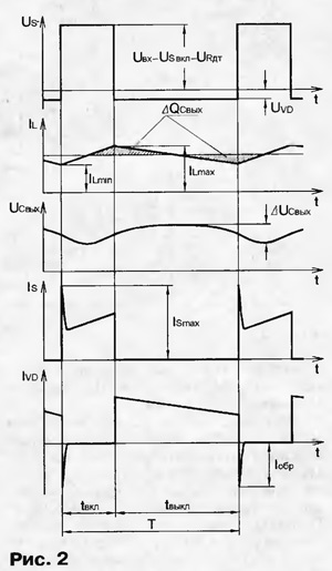
At time t on, the electronic switch S is closed and the current flows through the circuit: the positive terminal of the capacitor C in, the resistive current sensor R dt, the storage inductor L, the capacitor C out, the load, the negative terminal of the capacitor C in. At this stage, the inductor current l L is equal to the current of the electronic switch S and increases almost linearly from l Lmin to l Lmax .
According to a mismatch signal from the comparison node or an overload signal from a current sensor, or a combination of them, the generator switches the electronic switch S to an open state. Since the current through the inductor L cannot change instantly, then under the action of the self-induction EMF, the diode VD opens and the current l L will flow along the circuit: the cathode of the diode VD, the inductor L, the capacitor C VX, the load, the anode of the diode VD. At time t lKl, when the electronic switch S is open, the inductor current l L coincides with the diode current VD and decreases linearly from
l Lmax to l L min . During the Period T, the capacitor C out receives and gives an increment of charge ΔQ out. corresponding to the shaded area on the time diagram of the current l L . This increment determines the amplitude of the ripple voltage ΔU Cout on the capacitor Cout and on the load.
When the electronic switch is closed, the diode closes. This process is accompanied by a sharp increase in the switch current to the value of I smax due to the fact that the resistance of the circuit ≈ current sensor, closed switch, recovery diode ≈ is very small. To reduce dynamic losses, diodes with a short reverse recovery time should be used. In addition, the buck regulator diodes must be able to handle large reverse current. With the restoration of the closing properties of the diode, the next conversion period begins.
If the switching buck regulator operates at a low load current, it can switch to the intermittent inductor current mode. In this case, the inductor current stops by the moment the switch is closed and its increase starts from zero. The intermittent current mode is undesirable at a load current close to the nominal one, since in this case increased output voltage ripple occurs. The most optimal situation is when the stabilizer operates in the continuous current mode of the inductor at maximum load and in the intermittent current mode, when the load decreases to 10 ... 20% of the nominal.
The output voltage is regulated by changing the ratio of the closed state time of the switch to the pulse repetition period. In this case, depending on the circuitry, various options for implementing the control method are possible. In devices with relay control, the transition from the switched on state to the switched off state determines the comparison node. When the output voltage is greater than the set value, the switch is turned off, and vice versa. If you fix the pulse repetition period, then the output voltage can be adjusted by changing the duration of the switched on state of the switch. Sometimes methods are used in which either the time of the closed or the time of the open state of the switch is fixed. In any of the control methods, it is necessary to limit the inductor current at the stage of the closed state of the switch to protect against output overload. For these purposes, a resistive sensor or a pulse current transformer is used.
Calculation of a switching buck regulator
The choice of the main elements of a pulsed step-down stabilizer and the calculation of their modes will be carried out using a specific example. All the ratios that are used in this case are obtained on the basis of the analysis of the functional diagram and timing diagrams, and the methodology is taken as the basis.
1. Based on a comparison of the initial parameters and the maximum allowable current and voltage values of a number of powerful transistors and diodes, we first select a bipolar composite transistor KT853G (electronic switch S) and a diode KD2997V (VD).
2. Calculate the minimum and maximum fill factors:
γ min \u003d t and min / T min \u003d (U VyX + U pr) / (U BX max + U s on ≈ U RdT + U pr) \u003d (12 + 0.8) / (32-2-0.3 + 0.8)=0.42;
γ max \u003d t and max / T max \u003d (U Bvyx + U pp) / (U Bx min - U sbkl -U Rdt + U pp) \u003d (12 + 0.8) / (18-2-0.3 + 0.8)=0.78, where U pr =0.8 V ≈ direct voltage drop across the diode VD, obtained from the direct branch of the I–V characteristic for a current equal to I V in the worst case; U sbcl \u003d 2 V ≈ saturation voltage of the KT853G transistor, which acts as a switch S, with a current transfer coefficient in saturation mode h 21e \u003d 250; U RdT = 0.3 V ≈ voltage drop across the current sensor at rated load current.
3. Select the maximum and minimum conversion frequency.
This item is performed if the pulse period is not constant. We choose a control method with a fixed duration of the open state of the electronic switch. In this case, the following condition is fulfilled: t=(1 - γ max)/f min = (1 - γ min)/f max =const.
Since the switch is made on the KT853G transistor, which has poor dynamic characteristics, we will choose the maximum conversion frequency relatively low: f max =25 kHz. Then the minimum conversion frequency can be defined as
f min \u003d f max (1 - γ max) / (1 - γ min) \u003d 25 * 10 3 ] (1 - 0.78) / (1-0.42) \u003d 9.48 kHz.
4. Calculate the power loss on the switch.
Static losses are determined by the effective value of the current flowing through the switch. Since the current shape is ≈ trapezoid, then I s \u003d I out where α \u003d l Lmax / l lx \u003d 1.25 ≈ the ratio of the maximum inductor current to the output current. Coefficient a is chosen within 1.2 ... 1.6. Switch static losses P Sstat =l s U SBKn =3.27-2=6.54 W.
Dynamic losses on the switch Р sdyn ╥0.5f max ╥U BX max (l smax ╥t f +α╥l lx ╥t cn),
where I smax ≈ the switch current amplitude due to the reverse recovery of the VD diode. Taking l Smax =2l ByX , we obtain
R sdin \u003d 0.5f max ╥U BX max ╥I out (2t f + α∙ t cn) \u003d 0.5╥ 25╥10 3 ╥32╥5 (2╥0.78-10 -6 +1.25 -2-10 -6)=8.12 W, where t f =0.78╥10 -6 s ≈ the duration of the front of the current pulse through the switch, t cn =2╥10 -6 s ≈ the duration of the decline.
The total losses on the switch are: P s \u003d P scstat + P sdin \u003d 6.54 + 8.12 \u003d 14.66 W.
If static losses prevailed on the switch, the calculation should be carried out for the minimum input voltage when the inductor current is maximum. In the case where it is difficult to predict the predominant type of losses, they are determined both at the minimum and at the maximum input voltage.
5. We calculate the power loss on the diode.
Since the shape of the current through the diode ≈ is also a trapezoid, we define its effective value as Static losses on the diode P vDcTaT \u003d l vD ╥U pr \u003d 3.84-0.8 \u003d 3.07 W.
The dynamic losses of the diode are mainly due to losses during reverse recovery: P VDdyn \u003d 0.5f max ╥
l smax vU Bx max ╥t oB ╥f max ╥l Bыx ╥U in max ╥t ov ╥25-10 3 -5-32╥0.2╥10 -6 =0.8 W, where t OB =0, 2-1C -6 s ≈ diode reverse recovery time.
The total losses on the diode will be: P VD \u003d P MDstat + P VDdin \u003d 3.07 + 0.8 \u003d 3.87 W.
6. Choose a heat sink.
The main characteristic of a heat sink is its thermal resistance, which is defined as the ratio between the temperature difference between the environment and the heat sink surface to the power dissipated by it: R g = ΔT / P rass. In our case, it is necessary to fix the switching transistor and the diode on the same heat sink through insulating spacers. In order not to take into account the thermal resistance of the gaskets and not complicate the calculation, we choose a low surface temperature, approximately 70 degrees. C. Then at ambient temperature 40╟СΔТ=70-40=30╟С. The thermal resistance of the heat sink for our case R t \u003d ΔT / (P s + P vd) \u003d 30 / (14.66 + 3.87) \u003d 1.62╟С / W.
Thermal resistance during natural cooling is given, as a rule, in the reference data for the heat sink. To reduce the size and weight of the device, you can apply forced cooling with a fan.
7. Calculate the throttle parameters.
Let's calculate the inductance of the inductor: L= (U BX max - U sbkl -U Rdt - U Out)γ min /=(32-2-0.3-12)╥0.42/=118.94 μH.
As the material of the magnetic core, we choose pressed Mo-permalloy MP 140. The variable component of the magnetic field in the magnetic circuit in our case is such that hysteresis losses are not a limiting factor. Therefore, the maximum induction can be chosen on the linear section of the magnetization curve near the inflection point. Work on a curved section is undesirable, since in this case the magnetic permeability of the material will be less than the initial one. This in turn will cause the inductance to decrease as the inductor current increases. We choose the maximum induction B m equal to 0.5 T and calculate the volume of the magnetic circuit: Vp \u003d μμ 0 ╥L (αI outx) 2 / B m 2 \u003d 140 ╥ 4π ╥ 10 -7 ╥ 118.94 ╥ 10 -6 (1.25 -5) 2 0.5 2 \u003d 3.27 cm 3, where μ \u003d 140 ≈ initial magnetic permeability of the MP140 material; μ 0 =4π╥10 -7 H/m ≈ magnetic constant.
According to the calculated volume, we select the magnetic circuit. Due to the design features, the MP140 permalloy magnetic circuit is usually performed on two folded rings. In our case, rings KP24x13x7 are suitable. The cross-sectional area of the magnetic circuit Sc=20.352 =0.7 cm 2, and the average length of the magnetic line λс=5.48 cm. The volume of the selected magnetic circuit is: VC=SC╥ λс=0.7╥5.48=3.86 cm 3 >VP.
We calculate the number of turns: We take the number of turns equal to 23.
We determine the diameter of the wire with insulation based on the fact that the winding must fit in one layer, turn to turn along the inner circumference of the magnetic circuit: where d K \u003d 13 mm ≈ the inner diameter of the magnetic circuit; k 3 \u003d 0.8 ≈ filling factor of the magnetic circuit window with a winding.
We select the wire PETV-2 with a diameter of 1.32 mm.
Before winding the wire, the magnetic core should be insulated with a PET-E film 20 µm thick and 6...7 mm wide in one layer.
8. Calculate the capacitance of the output capacitor: C Bvyx \u003d (U BX max -U sBcl - U Rdt) ╥γ min /= (32-2-0.3) 0.42 / \u003d 1250 μF, where ΔU Сvyx \u003d 0, 01 V ≈ peak-to-peak ripple on the output capacitor.
The above formula does not take into account the influence of the internal, series resistance of the capacitor on the ripple. With this in mind, as well as a 20% tolerance for the capacitance of oxide capacitors, we select two K50-35 capacitors for a nominal voltage of 40 V with a capacity of 1000 microfarads each. The choice of capacitors with an overestimated rated voltage is due to the fact that with an increase in this parameter, the series resistance of the capacitors decreases.
The scheme developed in accordance with the results obtained in the course of the calculation is shown in fig. 3.
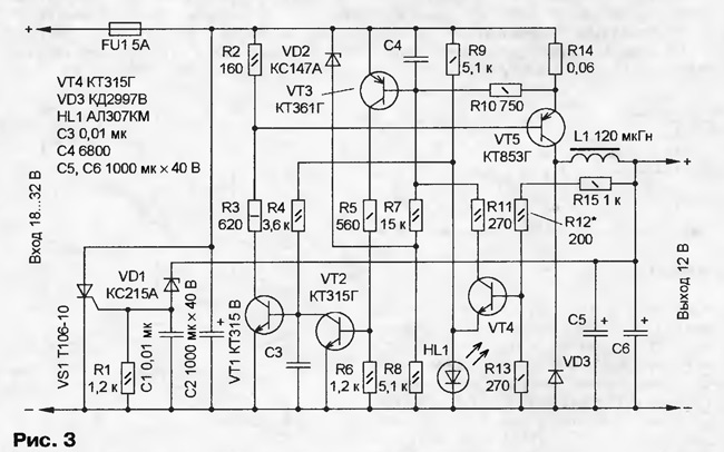
Let's consider the stabilizer in more detail. During the open state of the electronic switch ≈ transistor VT5 ≈ a sawtooth voltage is formed on the resistor R14 (current sensor). When it reaches a certain value, the transistor VT3 will open, which, in turn, will open the transistor VT2 and discharge the capacitor C3. In this case, the transistors VT1 and VT5 will close, and the switching diode VD3 will also open. The previously open transistors VT3 and VT2 will close, but the transistor VT1 will not open until the voltage across the capacitor C3 reaches a threshold level corresponding to its opening voltage. Thus, a time interval will be formed during which the switching transistor VT5 will be closed (approximately 30 μs). At the end of this interval, transistors VT1 and VT5 will open and the process will repeat again.
Resistor R. 10 and capacitor C4 form a filter that suppresses the voltage surge at the base of the transistor VT3 due to the reverse recovery of the diode VD3.
For silicon transistor VT3, the base≈emitter voltage at which it switches to active mode is about 0.6 V. In this case, relatively large power is dissipated on the current sensor R14. To reduce the voltage on the current sensor, at which the transistor VT3 opens, a constant bias of about 0.2 V is applied to its base along the VD2R7R8R10 circuit.
A voltage proportional to the output voltage is supplied to the base of the transistor VT4 from a divider, the upper arm of which is formed by resistors R15, R12, and the lower arm is ≈ resistor R13. The HL1R9 circuit generates a reference voltage equal to the sum of the direct voltage drop across the LED and the emitter junction of the transistor VT4. In our case, the exemplary voltage is 2.2 V. The mismatch signal is equal to the difference between the voltage at the base of the VT4 transistor and the exemplary one.
The output voltage is stabilized due to the summation of the mismatch signal amplified by the transistor VT4 with the voltage based on the transistor VT3. Assume that the output voltage has increased. Then the voltage at the base of the transistor VT4 will become more exemplary. Transistor VT4 opens slightly and shifts the voltage at the base of transistor VT3 so that it also starts to open. Consequently, the transistor VT3 will open at a lower level of the sawtooth voltage across the resistor R14, which will lead to a reduction in the time interval at which the switching transistor will be open. The output voltage will then decrease.
If the output voltage decreases, the regulation process will be similar, but occurs in the reverse order and leads to an increase in the open time of the switch. Since the current of the resistor R14 is directly involved in the formation of the open time of the transistor VT5, here, in addition to the usual output voltage feedback, there is a current feedback. This allows you to stabilize the output voltage without load and provide a quick response to a sudden change in current at the output of the device.
In the event of a short circuit in the load or overload, the stabilizer switches to current limiting mode. The output voltage begins to decrease at a current of 5.5 ... 6 A, and the closing current is approximately equal to 8 A. In these modes, the on-time of the switching transistor is reduced to a minimum, which reduces the power dissipated on it.
If the stabilizer does not work properly, caused by the failure of one of the elements (for example, a breakdown of the transistor VT5), the voltage increases at the output. In this case, the load may fail. To prevent emergency situations, the converter is equipped with a protection unit, which consists of a trinistor VS1, a zener diode VD1, a resistor R1 and a capacitor C1. When the output voltage exceeds the stabilization voltage of the zener diode VD1, a current begins to flow through it, which turns on the trinistor VS1. Its inclusion leads to a decrease in the output voltage to almost zero and blown fuse FU1.
The device is designed to power 12-volt audio equipment, designed mainly for passenger vehicles, from the on-board network of trucks and buses with a voltage of 24 V. Due to the fact that the input voltage in this case has a low ripple level, capacitor C2 has a relatively small capacitance. It is insufficient when the stabilizer is powered directly from the mains transformer with a rectifier. In this case, the rectifier should be equipped with a capacitor with a capacity of at least 2200 microfarads for the corresponding voltage. The transformer must have an overall power of 80 ... 100 W.
The stabilizer uses oxide capacitors K50-35 (C2, C5, C6). Capacitor SZ ≈ film K73-9, K73-17, etc. of suitable sizes, C4 ≈ ceramic with low self-inductance, for example, K10-176. All resistors, except R14, ≈ C2-23 of the corresponding power. Resistor R14 is made of a 60 mm long piece of PEC 0.8 constantan wire with a linear resistance of approximately 1 ohm/m.
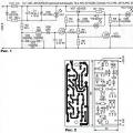
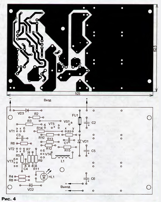
A drawing of a printed circuit board made of one-sided foil-coated fiberglass is shown in fig. 4.
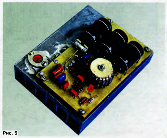
Diode VD3, transistor VD5 and trinistor VS1 are attached to the heat sink through an insulating heat-conducting gasket using plastic bushings. The board is also fixed on the same heat sink.
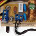
The appearance of the assembled device is shown in Fig. 5.
LITERATURE
1. Titze W., Shenk K. Semiconductor circuitry: A reference guide. Per. with him. ≈ M.: Mir, 1982.
2. Semiconductor devices. Transistors of medium and high power: a Handbook / A. A. Zaitsev, A. I. Mirkin, V. V. Mo-kryakov, etc. Ed. A. V. Golomedova. ≈ M.: Radio and communication, 1989.
3. Semiconductor devices. Rectifier diodes, zener diodes, thyristors: Handbook / A. B. Gitsevich, A. A. Zaitsev, V. V. Mokryakov, etc. Ed. A. V. Golomedova. ≈ M.: Radio and communication, 1988.