Adjustable power supply from an ATX computer power supply
(ATH - this is with the duty room)
There is a lot of information on the Internet about converting the power supply unit (PSU) from an AT and ATX computer. But I decided to highlight the most important information and compose my own article from everything that I found on the Internet specifically for the site
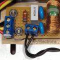
First of all, we look at the quality of the power supply assembled by the “Chinese)))”. A normal power supply should look something like this
What you should pay attention to is the high-voltage part of the power supply. There should be smoothing capacitors and chokes (They smooth out the pulse surge into the network), it should also be at least 2A for the diode bridge and capacitors after the bridge (I usually set 680 µF/200V or 330 µF/200V based on the required power) , if you want to get 300 W (30V/10A) from a power supply, then you need to set at least 600 uF.
Naturally, you need to pay attention to the power switches Q1-2 and the damper circuit C8R4. Q1-2 is usually set to MJE13007- MJE13009 (There are also articles about converting the circuit for field-effect transistors). Damper circuit C8R4, I noticed that when adjusting the power supply unit R4 of this circuit gets very hot, I decided to select C8.
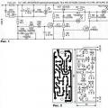
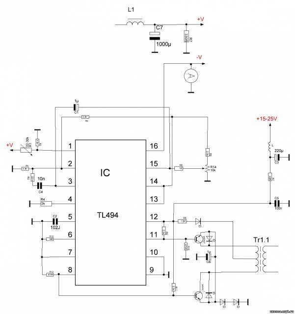
Next, the reworking of the power supply unit must be continued with a careful study of the circuit diagram of the power supply unit itself (although the circuit diagrams are almost the same, but it’s still worthwhile); all subsequent work depends on this. It is necessary to pay special attention to several things in studying the circuit: protection system (4th pin of the PWM controller), Power Good system (you can simply remove it), current error amplifier (15,16,3 PWM pins), current error amplifier voltage (1,2,3 PWM pins) and also the output circuit of the power supply (Here you will need to redo everything).
Let's consider each point in order.
Protection systems (4th pin) The diagram is taken from Golubev’s article drive2.ru
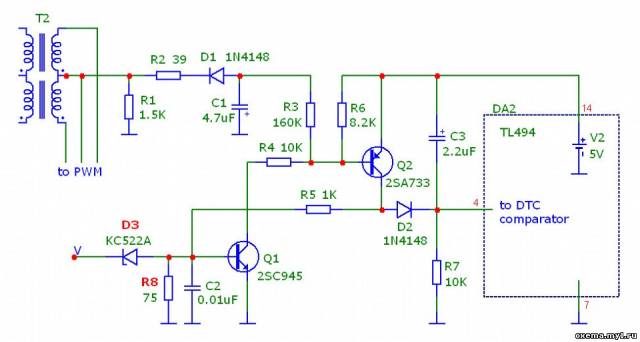
This is a typical scheme (Although there are others) of what is happening here. When the load on the inverter increases above the permissible limit, the pulse width at the middle terminal of the isolation transformer T2 increases. Diode D1 detects them, and the negative voltage across capacitor C1 increases. Having reached a certain level (approximately -11 V), it opens transistor Q2 through resistor R3. A voltage of +5 V will flow through an open transistor to pin 4 of the controller and stop the operation of its pulse generator.
All diodes and resistors suitable from the secondary rectifiers to the Q1 base are unsoldered from the circuit, and a zener diode D3 is installed at a voltage of 22 V (or higher voltage), for example, KS522A, and resistor R8.
In the event of an emergency increase in voltage at the output of the power supply above 22 V, the zener diode will break through and open transistor Q1. This, in turn, will open transistor Q2, through which a voltage of +5 V will be supplied to pin 4 of the controller, and will stop the operation of its pulse generator.
If you do not need protection, then you can simply unsolder everything and short-circuit pin 4 to the case through a resistor (the circuit will be below).
Power system Good - I usually just solder it.
Current error amplifier (15,16,3 PWM pins) - this is the adjustment of the output current. But this does not mean that you don’t have to worry about protection from short circuits.
Voltage error amplifier (1,2,3 PWM pins) - This is the output voltage adjustment.
And so is the voltage regulation.
(Immediately the protection diagram)
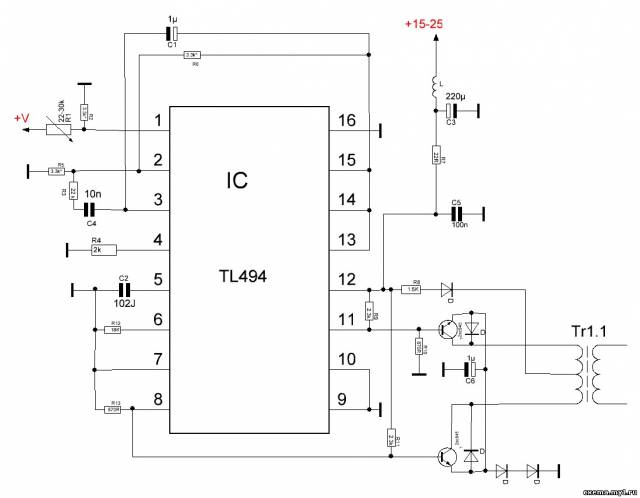
This circuit is designed without current regulation.
The 14th PWM pin is the reference voltage. And pins 2.1 are the voltage input of the op-amp.
All adjustments are made using voltage dividers. We apply the reference voltage to pin 2 from pin 14 through a 3.3 kOhm divider R5R6. This divider is designed for a voltage of 2.4V. Next, we need to apply the output voltage from the secondary circuit to the first PWM pin and also through a divider, but through an alternating one. Variable resistor R1 and constant resistor R3. On my power supply there was an adjustment from 2-24 Volts. The output voltage also depends on the power transformer and the output circuit, but more on that later. Let's return to our Shimka, setting up the voltage regulation does not end there. We also need to pay attention to the 3rd pin of the PWM, this is the output of the op-amp and it needs to be made OOS on the 2nd leg for smooth adjustment and to remove noise, crackling and other unpleasant sound of the transformer. I have it assembled on C4R3 and C1. Although C4R3 is often enough, but due to the wide variety of “Chinese manufacturers”, you sometimes need to add a capacitor, usually 1 µF is enough, but sometimes it reaches 5 µF.
Circuits C4R3 and C1 need to be selected so that there is no noise in the transmission, but if it still remains, then you need to pay attention to the secondary circuit inductor, there may be a violation of the core, but we will talk about this later.
Yes, about the protection, I removed it here and installed a 2 kOhm resistor R4.
Now about adjusting the current
In principle, current regulation is also voltage regulation. Using a divider, but only here the reference voltage changes and the voltage drop across the ammeter (or shunt) is monitored. In principle, there is nothing new regarding voltage regulation, only C1 is required and perhaps a resistor will need to be added in series, but this already depends on the PWM and Tr-ra.
The general adjustment circuit is 100% workable and has been proven in practice; if your circuit does not work stably or is not quite correct, then you need to: 1. Select the ratings for your PWM and parameters, 2. Look for errors in the assembly and modify it. Again, I repeat, practice has shown that Chinese PWM and power supply units generally react differently to changes in circuits. Everything needs to be configured using the method of selection and calculations.
In the ATX power supply unit, the PWM and isolation transformer are powered from the standby power supply; it can reach 25 V and is supplied to the 12th PWM pin circuit. Many people believe that the diode in the secondary circuit of the Power TR-RA going to pin 12 needs to be removed. I believe that it is better to leave this circuit; this gives additional confidence that the power switches will be preserved when their standby power fails.
Now about the secondary circuit
The best conversion scheme seemed to me to be S. Golubeva (Driver2.ru)
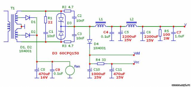
Although the fan cannot be hung on a five-volt winding, because the voltage will also change there, and there is still no feedback from the PWM, and therefore, under a load with a current of 0.15A, the voltage will drop noticeably.
Now about the output voltage circuit itself. There is no point in changing the pinout of the transmitter and installing a diode bridge. Because voltage increases and power decreases. Therefore, I prefer this scheme, and then there are fewer alterations. Rectifier diodes D3 must have a current of at least 10 A and a reverse voltage of at least 200 Volts. These could be STPR1020CT,F12C20.ER1602CT. Diode D4 is (as I call it) the auxiliary PWM power supply circuit and Vcc and Vdd protection. If you wish, you can leave the L1 ring inductance as the old one (If, of course, it works normally), but I rewind it with the same wire + a wire from a five-volt circuit. I usually leave inductance L2 unmeasured. Capacitors C5C6 should not be installed with a nominal value of more than 2200 uF; it makes no sense. I usually set it to 1000 microfarads and that’s enough. Non-polar C4C7 can be raised to 1 uF if desired, but I also did not see much of a difference. But resistor R5 should not be set to less than 300 Ohms; it will simply heat up at a voltage of more than 10 V, but not more than 500 Ohms. This resistor balances the power supply, so to speak.
This is actually the most important thing in remaking the power supply.
Again, I would like to draw your attention to the fact that not all power supplies can be easily and simply redesigned and customized. Therefore, you need to carefully study the diagram and information on the alteration.