PULSE POWER SUPPLY UNIT FOR TL494 AND IR2110
Most automotive and network voltage converters are based on a specialized TL494 controller and since it is the main one, it would not be fair not to briefly tell about the principle of its operation.
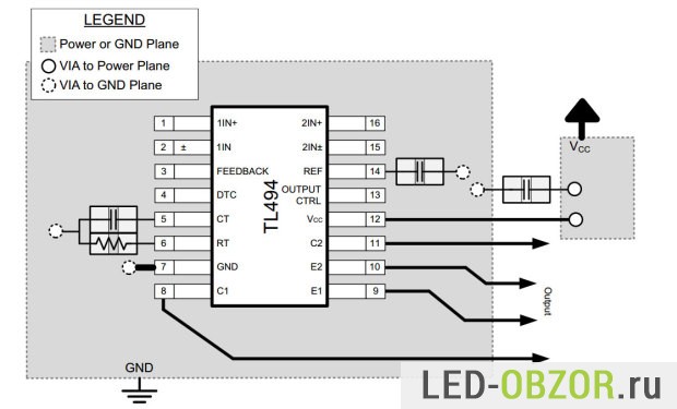
The TL494 controller is a DIP16 plastic case (there are variants in a planar case, but it is not used in these designs). The functional diagram of the controller is shown in Fig. 1.

Picture 1 - Structural scheme chips TL494.
As you can see from the figure, the TL494 microcircuit has very developed control circuits, which makes it possible to build converters on its basis for almost any requirements, but first, a few words about the functional units of the controller.
ION and undervoltage protection circuits.
The circuit turns on when the power supply reaches the threshold of 5.5..7.0 V (typical value 6.4V). Until this moment, the internal control buses inhibit the operation of the generator and the logic part of the circuit. No-load current at supply voltage + 15V (output transistors are disabled) no more than 10 mA. ION + 5V (+4.75 .. + 5.25 V, output stabilization not worse than +/- 25 mV) provides a flowing current of up to 10 mA. It is possible to power up the reference only by using an npn emitter follower (see TI pages 19-20), but at the output of such a "stabilizer" the voltage will strongly depend on the load current.
Generator generates on the timing capacitor Сt (pin 5) a sawtooth voltage of 0 .. + 3.0V (the amplitude is set by the ION) for TL494 Texas Instruments and 0 ... + 2.8V for TL494 Motorola (what can we expect from others?), respectively for TI F = 1.0 / (RtCt), for Motorola F = 1.1 / (RtCt).
Operating frequencies allowed
from 1 to 300 kHz, while the recommended range is Rt = 1 ... 500 kΩ, Ct = 470pF ... 10μF. In this case, the typical temperature drift of the frequency is (naturally, without taking into account the drift of the attached components) +/- 3%, and the frequency drift, depending on the supply voltage, is within 0.1% in the entire permissible range.
For remote shutdown
generator, you can use an external key to close the input Rt (6) to the output of the ION, or - close Ct to the ground. Of course, the leakage resistance of the open switch must be taken into account when choosing Rt, Ct.
Rest phase control input
(duty cycle) through the quiescent phase comparator sets the required minimum pause between pulses in the arms of the circuit. This is necessary both to prevent through current in the power stages outside the IC, and to ensure stable operation of the trigger - the switching time of the digital part of the TL494 is 200 ns. The output signal is enabled when the saw at CT exceeds the voltage at control input 4 (DT). At clock frequencies up to 150 kHz with zero control voltage, the quiescent phase = 3% of the period (equivalent displacement of the control signal 100..120 mV), at high frequencies the built-in correction extends the quiescent phase to 200..300 ns.
By using the DT input circuit, it is possible to set a fixed quiescent phase (R-R divider), soft start mode (R-C), remote shutdown (key), and also use DT as a linear control input. The input circuit is assembled on pnp transistors, so the input current (up to 1.0 μA) flows out of the IC and does not flow into it. The current is large enough, so high-resistance resistors (no more than 100 kΩ) should be avoided. See TI, page 23 for an example of overvoltage protection using a TL430 3-lead Zener diode (431).
Error amplifiers
- in fact, operational amplifiers with Ku = 70..95 dB at constant voltage (60 dB for early series), Ku = 1 at 350 kHz. The input circuits are based on pnp transistors, so the input current (up to 1.0 μA) flows out of the IC rather than flows into it. The current is large enough for the op-amp, the bias voltage is also (up to 10 mV), so high-resistance resistors in the control circuits (no more than 100 kΩ) should be avoided. But thanks to the use of pnp-inputs, the input voltage range is from -0.3V to Vpower-2V
When using an RC frequency-dependent operating system, remember that the output of the amplifiers is actually a single-ended (serial diode!), So it will charge the capacitor (up), and it will take a long time to discharge downward. The voltage at this output is in the range of 0 .. + 3.5V (slightly more than the oscillator swing), then the voltage coefficient drops sharply and at about 4.5V at the output the amplifiers saturate. Likewise, low impedance resistors should be avoided in the output circuits of amplifiers (feedback loops).
Amplifiers are not designed to operate within a single clock cycle. With a signal propagation delay of 400 ns inside the amplifier, they are too slow for this, and the trigger control logic does not allow (there would be side pulses at the output). In real PN circuits, the cutoff frequency of the feedback circuit is chosen to be of the order of 200-10000 Hz.
Trigger and output control logic
- With a supply voltage of at least 7V, if the saw voltage at the generator is greater than at the control input DT, and if the saw voltage is higher than at any of the error amplifiers (taking into account the built-in thresholds and offsets), the circuit output is allowed. When the generator is reset from maximum to zero, the outputs are disabled. A trigger with a paraphase output divides the frequency in half. With a logic 0 at input 13 (output mode), the trigger phases are ORed and fed simultaneously to both outputs, with a logic 1, they are fed in paraphase to each output separately.
Output transistors
- npn Darlingtons with built-in thermal protection (but no overcurrent protection). Thus, the minimum voltage drop between the collector (usually closed to the positive rail) and the emitter (at the load) is 1.5V (typical at 200 mA), and in a circuit with a common emitter, it is slightly better, 1.1 V typical. The maximum output current (with one open transistor) is limited to 500 mA, the maximum power for the entire crystal is 1W.
Switching power supplies are gradually replacing their traditional relatives in sound engineering, since they look noticeably more attractive both economically and overall. The same factor that switching power supplies contribute to the distortion of the amplifier, namely, the appearance of additional overtones is already losing its relevance mainly for two reasons - the modern element base allows you to design converters with a conversion frequency significantly higher than 40 kHz, hence the power supply modulation introduced by the power supply will already be in ultrasound. In addition, a higher power frequency is much easier to filter out, and the use of two L-shaped LC filters in the power supply circuits already sufficiently smooths out the ripple at these frequencies.
Of course, there is also a fly in the ointment in this barrel of honey - the difference in price between a typical power supply for a power amplifier and a pulsed one becomes more noticeable with an increase in the power of this unit, i.e. the more powerful the power supply, the more profitable it is in relation to its standard counterpart.
And that is not all. Using switching power supplies, it is necessary to adhere to the rules for installing high-frequency devices, namely, the use of additional screens, the supply of a common wire to the heat sinks of the power section, as well as the correct wiring of the ground and the connection of shielding braids and conductors.
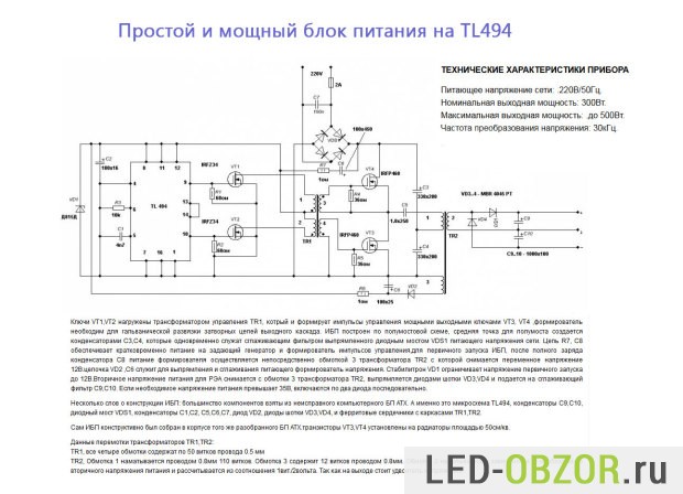
After a small lyrical digression about the features of switching power supplies for power amplifiers, there is a schematic diagram of a 400W power supply:
Picture 1. Schematic diagram switching power supply for power amplifiers up to 400 W
INCREASE IN GOOD QUALITY
The TL494 serves as the control controller in this power supply. Of course, there are more modern microcircuits for this task, however, we use this particular controller for two reasons - it is VERY easy to purchase. For quite a long time, the TL494 from Texas Instruments was used in the manufactured power supplies, no quality problems were found. The error amplifier is covered by OOS, which allows you to achieve a fairly large coffee. stabilization (the ratio of resistors R4 and R6).
After the TL494 controller, there is an IR2110 half-bridge driver, which actually controls the gates of the power transistors. The use of the driver made it possible to abandon the matching transformer, which is widely used in computer power supplies. The IR2110 driver is loaded on the gates through the R24-VD4 and R25-VD5 chains accelerating the closing of the field drivers.
Power switches VT2 and VT3 operate on the primary winding of the power transformer. The midpoint required to obtain an alternating voltage in the primary winding of the transformer is formed by elements R30-C26 and R31-C27.
A few words about the algorithm of operation of the switching power supply unit on the TL494:
At the moment the 220 V mains voltage is applied, the capacitances of the primary power supply filters C15 and C16 become infected through the resistors R8 and R11, which does not allow the VD diol bridge to overload with a short-circuit current of completely discharged C15 and C16. At the same time, capacitors C1, C3, C6, C19 are charged through a line of resistors R16, R18, R20 and R22, a stabilizer 7815 and a resistor R21.
As soon as the voltage on the capacitor C6 reaches 12 V, the Zener diode VD1 "breaks through" and a current begins to flow through it charging the capacitor C18, and as soon as the positive terminal of this capacitor reaches a value sufficient to open the thyristor VS2, it will open. This will result in the switching on of the relay K1, which by its contacts will bypass the current-limiting resistors R8 and R11. In addition, the opened thyristor VS2 will open the transistor VT1 to the TL494 controller and the IR2110 half-bridge driver. The controller will start the soft start mode, the duration of which depends on the values of R7 and C13.
During a soft start pulse duration, opening the power transistors increase gradually, thereby gradually charging the secondary power capacitors and limiting the current through the rectifier diodes. The duration increases until the amount of secondary power is sufficient to open the LED of the optocoupler IC1. As soon as the brightness of the optocoupler LED becomes sufficient to open the transistor, the pulse duration will stop increasing (Figure 2).

Figure 2. Soft start mode.
It should be noted here that the duration of the soft start is limited, since the current passing through the resistors R16, R18, R20, R22 is not enough to power the TL494 controller, IR2110 driver and the relay winding turned on - the supply voltage of these microcircuits will begin to decrease and soon decrease to a value at which TL494 will stop generating control pulses. And it is up to this moment that the soft start mode must be terminated and the converter must return to normal operating mode, since the TL494 controller and the IR2110 driver receive the main power from the power transformer (VD9, VD10 is a midpoint rectifier, R23-C1-C3 is an RC filter, IC3 is a 15 V regulator) and that is why capacitors C1, C3, C6, C19 have such large ratings - they must maintain the controller's power supply until it enters normal operation.
The TL494 stabilizes the output voltage by changing the duration of the control pulses of the power transistors at a constant frequency - Width and pulse M modulation - PWM... This is possible only if the value of the secondary voltage of the power transformer is higher than that required at the output of the stabilizer by at least 30%, but not more than 60%.

Figure 3. The principle of operation of the PWM stabilizer.
With an increase in the load, the output voltage begins to decrease, the LED of the optocoupler IC1 starts to glow less, the optocoupler transistor closes, decreasing the voltage at the error amplifier and thereby increasing the duration of the control pulses until the operating voltage reaches the stabilization value (Figure 3). With decreasing load, the voltage will begin to increase, the LED of the optocoupler IC1 will begin to glow brighter, thereby opening the transistor and reducing the duration of the control pulses until the value of the effective value of the output voltage decreases to a stabilized value. The value of the stabilized voltage is regulated by the trimmer R26.
It should be noted that the TL494 controller does not regulate the duration of each pulse depending on the output voltage, but only the average value, i.e. the measuring part has some inertia. However, even with installed capacitors in the secondary power supply with a capacity of 2200 uF, the power supply dips during peak short-term loads do not exceed 5%, which is quite acceptable for HI-FI equipment. We usually put capacitors in the secondary power supply of 4700 uF, which gives a confident margin for peak values, and the use of a group stabilization inductor allows us to control all 4 output power voltages.
This switching power supply is equipped with overload protection, the measuring element of which is the current transformer TV1. As soon as the current reaches a critical value, the thyristor VS1 opens and bypasses the power supply of the final stage of the controller. The control pulses disappear and the power supply goes into standby mode, in which it can be for quite a long time, since the thyristor VS2 remains open - the current flowing through the resistors R16, R18, R20 and R22 is enough to keep it open. How to calculate a current transformer.
To remove the power supply from standby mode, you must press the SA3 button, which will bypass the thyristor VS2 with its contacts, the current will stop flowing through it and it will close. As soon as the contacts SA3 open, the transistor VT1 closes itself, removing power from the controller and driver. Thus, the control circuit will go into the minimum consumption mode - the thyristor VS2 is closed, therefore the relay K1 is off, the transistor VT1 is closed, therefore the controller and the driver are de-energized. Capacitors C1, C3, C6 and C19 begin to charge and as soon as the voltage reaches 12 V, the thyristor VS2 opens and the switching power supply unit starts up.
If you need to put the power supply into standby mode, you can use the SA2 button, when you press it, the base and emitter of the VT1 transistor will be connected. The transistor will close and de-energize the controller and driver. Control pulses disappear, disappear and secondary voltages... However, the power will not be removed from the K1 relay and the converter will not be restarted.
This circuitry makes it possible to assemble power supplies from 300-400 W to 2000 W, of course, that some elements of the circuit will have to be replaced, since in their parameters they simply cannot withstand heavy loads.
When assembling more powerful options, you should pay attention to the capacitors of the smoothing filters of the primary power supply C15 and C16. The total capacity of these capacitors must be proportional to the power of the power supply and correspond to the proportion of 1 W of the output power of the voltage converter corresponds to 1 μF of the capacitance of the primary power supply filter. In other words, if the power of the power supply is 400 W, then 2 capacitors of 220 μF should be used, if the power is 1000 W, then 2 capacitors of 470 μF or two of 680 μF must be installed.
This requirement has two purposes. First, the ripple decreases primary voltage power supply, which makes it easier to stabilize the output voltage. Secondly, the use of two capacitors instead of one facilitates the work of the capacitor itself, since electrolytic capacitors of the TK series are much easier to get, and they are not entirely intended for use in high-frequency power supplies - the internal resistance is too high and at high frequencies these capacitors will heat up. Using two pieces, the internal resistance is reduced, and the resulting heating is already divided between the two capacitors.
When used as power transistors IRF740, IRF840, STP10NK60 and similar ones (for more information about the most commonly used transistors in network converters, see the table at the bottom of the page), VD4 and VD5 diodes can be abandoned altogether, and the values of resistors R24 and R25 can be reduced to 22 Ohm - power the IR2110 driver is enough to control these transistors. If a more powerful switching power supply is being assembled, then more powerful transistors... Attention should be paid to both the maximum current of the transistor and its dissipation power - pulse stabilized power supplies are very sensitive to the correctness of the supplied supply and without it the power transistors heat up more, since currents formed through self-induction begin to flow through the diodes installed in the transistors. Learn more about choosing a snubber.
The closing time that increases without a supply is also not a small contribution to the heating - the transistor is in linear mode for a longer time.
Quite often they forget about another feature of field-effect transistors - with an increase in temperature, their maximum current decreases, and quite strongly. Based on this, when choosing power transistors for switching power supplies, you should have at least two times the maximum current for power amplifier power supplies and three times for devices operating on a large, unchanging load, for example, an induction smelter or decorative lighting, powering a low-voltage power tool.
The stabilization of the output voltage is carried out by means of the group stabilization choke L1 (DGS). Pay attention to the direction of the windings of this inductor. The number of turns should be proportional to the output voltages. Of course, there are formulas for calculating this winding unit, but experience has shown that the overall power of the core for DGS should be 20-25% of the overall power of the power transformer. You can wind it until the window is filled by about 2/3, not forgetting that if the output voltages are different, then the winding with a higher voltage should be proportionally larger, for example, you need two bipolar voltages, one at ± 35 V, and the second to power a subwoofer with a voltage ± 50 V.
We wind the DGS in four wires at once until 2/3 of the window is filled, counting the turns. The diameter is calculated based on a current strength of 3-4 A / mm2. Let's say we got 22 turns, make up the proportion:
22 turns / 35 V = X turns / 50 V.
X turns = 22 × 50/35 = 31.4 ≈ 31 turns
Next, cut off two wires for ± 35 V and wind up another 9 turns for a voltage of ± 50.
ATTENTION! Remember that the quality of stabilization directly depends on how quickly the voltage changes to which the diode of the optocoupler is connected. To improve coffee-stabilization, it makes sense to connect an additional load to each voltage in the form of 2 W resistors and 3.3 kΩ resistor. The load resistor connected to the voltage controlled by the optocoupler must be 1.7 ... 2.2 times less.
The winding data for mains switching power supplies on ferrite rings with a permeability of 2000 nm are summarized in Table 1.
CURRENT DATA FOR PULSE TRANSFORMERS |
||||||||||||||||||||
|
||||||||||||||||||||
|
||||||||||||||||||||
|
||||||||||||||||||||
|
||||||||||||||||||||
|
||||||||||||||||||||
|
||||||||||||||||||||
|
||||||||||||||||||||
|
||||||||||||||||||||
|
||||||||||||||||||||
|
||||||||||||||||||||
|
||||||||||||||||||||
|
||||||||||||||||||||
|
||||||||||||||||||||
However, it is far from always possible to recognize the brand of ferrite, especially if it is ferrite from line transformers of TVs. You can get out of the situation by finding out the number of turns empirically. More details about this in the video:
Using the above circuitry of the switching power supply, several sub-modifications were developed and tested, designed to solve a particular problem at various powers. Blueprints printed circuit boards ah of these power supplies are shown below.
Printed circuit board for a pulse stabilized power supply unit with a capacity of up to 1200 ... 1500 W. Board size 269x130 mm. In fact, this is a more advanced version of the previous PCB. Differs in the presence of a group stabilization choke that allows you to control the value of all power voltages, as well as an additional LC filter. Has fan control and overload protection. The output voltages consist of two bipolar power supplies and one bipolar low-current supply for the pre-stages.

Appearance printed circuit board of the power supply unit up to 1500 W. DOWNLOAD LAY
A stabilized switching power supply unit with a capacity of up to 1500 ... 1800 W can be performed on a printed circuit board with a size of 272x100 mm. The power supply is designed for a power transformer made on K45 rings and located horizontally. It has two bipolar power supplies that can be combined into one power supply for the amplifier with a bi-level power supply and one bipolar low-current supply for the preliminary stages.

Printed circuit board of a switching power supply unit up to 1800 W. DOWNLOAD LAY
This power supply can be used to power high-power automotive equipment, such as high-power car amplifiers, car air conditioners. The dimensions of the board are 188x123. The Schottky rectifier diodes used are parallelized by jumpers and the output current can reach 120 A at a voltage of 14 V. In addition, the power supply unit can supply a bipolar voltage with a load capacity of up to 1 A (installed integrated voltage stabilizers no longer allow). The power transformer is made on K45 rings, a filtering choke of power voltage on two K40x25x11 rings. Built-in overload protection.

Appearance of the printed circuit board of the power supply unit for automotive equipment DOWNLOAD LAY FORMAT
Power supply units up to 2000 W are made on two 275x99 boards located one above the other. The voltage is monitored by one voltage. Has overload protection. The file contains several variants of the "second floor" for two bipolar voltages, for two unipolar voltages, for voltages required for two and three level voltages. The power transformer is located horizontally and is made on the K45 rings.

External view of the "two-story" power supply DOWNLOAD LAY
The power supply unit with two bipolar voltages or one for a two-level amplifier is made on a 277x154 board. It has a group stabilization choke, overload protection. The power transformer is on the K45 rings and is located horizontally. Power up to 2000 W.

Appearance of the printed circuit board DOWNLOAD LAY
Almost the same power supply as above, but has one bipolar output voltage.

Appearance of the printed circuit board DOWNLOAD LAY
The switching power supply has two power bipolar stabilized voltages and one bipolar low current. Equipped with fan control and overload protection. Has a group stabilization choke and additional LC filters. Power up to 2000 ... 2400 W. The board measures 278x146 mm

Appearance of the printed circuit board DOWNLOAD LAY
The printed circuit board of a switching power supply for a power amplifier with two-level power supplies, 284x184 mm in size, has a group stabilization choke and additional LC filters, overload protection and fan control. Distinctive feature is the use of discrete transistors to speed up the closing of power transistors. Power up to 2500 ... 2800 W.

bi-level powered DOWNLOAD LAY
A slightly modified version of the previous PCB with two bipolar voltages. Size 285x172. Power up to 3000 W.
![]()
Exterior view of the printed circuit board of the power supply for the amplifier DOWNLOAD LAY
The bridge network switching power supply unit with a capacity of up to 4000 ... 4500 W is made on a printed circuit board with dimensions of 269x198 mm. It has two bipolar power voltages, fan control and overload protection. Uses a group stabilization choke. It is desirable to use external additional L filters of the secondary power supply.

Exterior view of the printed circuit board of the power supply for the amplifier DOWNLOAD LAY
There is much more space for ferrites on the boards than it could be. The fact is that it is not always necessary to go beyond the audio range. Therefore, additional areas are provided on the boards. Just in case, a small selection of reference data on power transistors and links where I would buy them. By the way, I have ordered TL494 and IR2110 more than once, and of course power transistors. True, he did not take the entire assortment, but no marriage has yet come across.
POPULAR TRANSISTORS FOR PULSE POWER SUPPLIES |
|||||||
NAME |
VOLTAGE |
POWER |
CAPACITY |
Qg |
|||
Most of the modern switching power supplies are made on TL494 microcircuits, which is a switching PWM controller. The power part is made on powerful elements, for example transistors. The TL494 connection circuit is simple, a minimum of additional radio components is required, the datasheet is described in detail.
Modification options: TL494CN, TL494CD, TL494IN, TL494C, TL494CI.
I also wrote reviews of other popular ICs,.
- 1. Characteristics and functionality
- 2. Analogs
- 3. Typical wiring diagrams for power supply units on TL494
- 4. Power supply diagrams
- 5. Conversion of ATX PSU to laboratory
- 6. Datasheet
- 7. Graphs of electrical characteristics
- 8. Functional microcircuit
Features and functionality
The TL494 microcircuit is designed as a PWM controller for switching power supplies with a fixed operating frequency. For setting the operating frequency, two additional external element resistor and capacitor. The microcircuit has a 5V reference voltage source, the error of which is 5%.
Application area indicated by the manufacturer:
- power supplies with a capacity of more than 90W AC-DC with PFC;
- microwaves;
- boost converters from 12V to 220V;
- power supplies for servers;
- inverters for solar panels;
- electric bicycles and motorcycles;
- down converters;
- smoke detectors;
- desktop computers.


Analogs

The most famous analogs of the TL494 chip are the domestic KA7500B, KR1114EU4 from Fairchild, Sharp IR3M02, UA494, Fujitsu MB3759. The wiring diagrams are similar, the pinout may be different.
The new TL594 is an analogue of the TL494 with increased accuracy comparator. TL598 analogue of TL594 with a repeater at the output.
Typical wiring diagrams for power supply units on TL494

The main switching circuits of the TL494 are collected from datasheets from various manufacturers. They can serve as a basis for the development of similar devices with similar functionality.
![]()
Power supply diagrams
I will not consider the complex circuits of the TL494 switching power supplies. They require a lot of parts and time, so it's not rational to make it yourself. It's easier from the Chinese to buy a ready-made similar module for 300-500 rubles.
When assembling step-up voltage converters, pay special attention to cooling the power transistors at the output. For 200W, the output will be about 1A, relatively not much. Perform stability testing with the maximum permissible load. The necessary load is best formed from incandescent lamps of 220 volts, 20w, 40w, 60w, 100w. Do not overheat the transistors by more than 100 degrees. Observe safety regulations when working with high voltages. Measure seven times, turn on once.
The boost converter on TL494 practically does not require adjustment, the repeatability is high. Check the resistor and capacitor ratings before assembly. The smaller the deviation, the more stable the inverter will work from 12 to 220 volts.
Temperature control of transistors is best done with a thermocouple. If the radiator is too small, it is easier to install a fan so as not to install a new radiator.
I had to make a power supply unit for TL494 with my own hands for a subwoofer amplifier in a car. At the time, 12V to 220V car inverters were not being sold and the Chinese did not have Aliexpress. As an amplifier, the ULF used an 80W TDA series microcircuit.
Over the past 5 years, interest in electrically driven technology has increased. This was facilitated by the Chinese, who began mass production of electric bicycles, modern wheel-motor with high efficiency. I think the best implementation is two-wheeled and one-wheeled hoverboards. In 2015, the Chinese company Ninebot bought the American Segway and began producing 50 types of electric scooters such as Segway.
A good control controller is required to control a powerful low voltage motor.

Converting an ATX PSU into a laboratory
Every radio amateur has a powerful unit ATX power supply from a computer that outputs 5V and 12V. Its power is from 200W to 500W. Knowing the parameters of the controlling controller, you can change the parameters of the ATX source. For example, increase the voltage from 12 to 30V. There are two popular ways, one from Italian radio amateurs.
Consider the Italian method, which is as simple as possible and does not require rewinding of transformers. The ATX output is completely removed and refined according to the diagram. A huge number of radio amateurs have repeated this scheme due to its simplicity. Output voltage from 1V to 30V, current up to 10A.
Datasheet
The microcircuit is so popular that it is produced by several manufacturers, offhand I found 5 different datasheets, from Motorola, Texas Instruments and other lesser known ones. The most complete datasheet TL494 from Motorola, which I will publish.
All datasheets, you can download each:
- Motorola;
- Texas Instruments
(not TDA1555, but more serious microcircuits), require a power supply unit with bipolar power supply... And the difficulty here arises just not in the UMZCH itself, but in a device that would increase the voltage to the required level, transferring a good current to the load. This converter is the hardest part of a homemade car amplifier. However, if you follow all the recommendations, you will be able to collect a verified PN according to this scheme, the scheme of which is given below. To enlarge - click on it.
The basis of the converter is a pulse generator built on a specialized widespread microcircuit. The generation frequency is set by the value of the resistor R3. You can change it to achieve the best stability and efficiency. Let's take a closer look at the device of the TL494 control microcircuit.
Parameters of the TL494 chip
Upit.chips (pin 12) - Upit.min = 9V; Upit.max = 40V
Permissible voltage at the input DA1, DA2 not more than Upit / 2
Valid parameters output transistors Q1, Q2:
Uns less than 1.3V;
Uke less than 40V;
Ik.max less than 250mA
The residual voltage of the collector-emitter of the output transistors is not more than 1.3V.
I consumed by the microcircuit - 10-12mA
Allowable power dissipation:
0.8W at an ambient temperature of + 25C;
0.3W at an ambient temperature of + 70C.
The frequency of the built-in reference generator is not more than 100 kHz.

- sawtooth voltage generator DA6; the frequency is determined by the values of the resistor and capacitor connected to the 5th and 6th pins;
- reference stabilized voltage source DA5 with an external output (pin 14);
- voltage error amplifier DA3;
- error amplifier for current limiting signal DA4;
- two output transistors VT1 and VT2 with open collectors and emitters;
- comparator "dead zone" DA1;
- comparator PWM DA2;
- dynamic push-pull D-trigger in the mode of frequency division by 2 - DD2;
- auxiliary logic gates DD1 (2-OR), DD3 (2nd), DD4 (2nd), DD5 (2-OR-NOT), DD6 (2-OR-NOT), DD7 (NOT);
- constant voltage source with a rating of 0.1B DA7;
- DC source with a rating of 0.7mA DA8.

Swing the load ( power transformer) field effect transistors IRFZ44N. Choke L1 is wound on a ferite ring with a diameter of 2 cm from computer unit nutrition. It contains 10 turns of a double wire with a diameter of 1 mm, which are distributed throughout the ring. If you do not have a ring, you can wind it on a ferite rod with a diameter of 8 mm and a length of a couple of centimeters (not critical). Layout of the board - download in.

We warn, the robotic capacity of the converter unit strongly depends on the correct manufacture of the transformer. It is wound on a ferite ring of the 2000NM brand with dimensions of 40 * 25 * 11 mm. First, you need to round off all the edges with a file, wrap it with linen tape. The primary winding is wound with a bundle that consists of 5 cores 0.7 mm thick and contains 2 * 6 turns, that is, 12. It winds like this: we take one core and wind it 6 turns evenly distributed around the ring, then we wind the next one close to the first and so on. 5 lived. At the terminals, the veins are twisted. Then, on the part of the ring free of wires, we begin to wind the second half of the primary winding in the same way. We get two equivalent windings. After that, we wrap the ring with electrical tape and wind the secondary winding with a 1.5mm wire 2 * 18 turns as well as the primary. So that nothing burns out during the first start, it is necessary to turn on through 100 Ohm resistors in each arm, and the transformer primary through a 40-60 W lamp, and everything will be buzzing even with random errors. A small addition: there is a small defect in the filter block circuit, the c19 r22 parts should be reversed, since when the phase rotates on the oscilloscope, the signal amplitude decays. In general, this step-up voltage converter can be safely recommended for repetition, since it has already been successfully assembled by many radio amateurs.